The intricate process of manufacturing Printed Circuit Boards involves several crucial stages, each contributing to the overall functionality and reliability of electronic devices. The journey begins with the translation of circuit schematics into a physical layout, a meticulous process that determines the PCB’s structure. Designers consider factors such as signal integrity, power distribution, and thermal management to optimize performance.
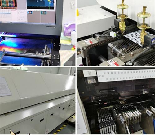
The fabrication phase is equally significant, involving the creation of conductive pathways using copper traces and insulating layers. Modern manufacturing techniques, like additive manufacturing and laser direct imaging, enhance precision and reduce production time. The final assembly stage sees electronic components strategically placed and soldered onto the board, marking the culmination of a precise and collaborative manufacturing effort.
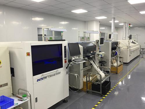
In recent years, eco-friendly practices have gained prominence in PCB manufacturing. Lead-free soldering and the use of recyclable materials align with global efforts toward sustainable electronics. Additionally, the rise of automated assembly lines and artificial intelligence in quality control ensures efficiency and consistency in mass production.
Understanding the intricacies of the PCB manufacturing process provides insight into the foundation of electronic devices. From design conceptualization to the final product, precision, and innovation define each stage, shaping the landscape of modern electronics.